Introduction To gEDA
Tutorial from the program creators can be found here. [1]
Open the program gEDA Schematic Editor. (gschem)
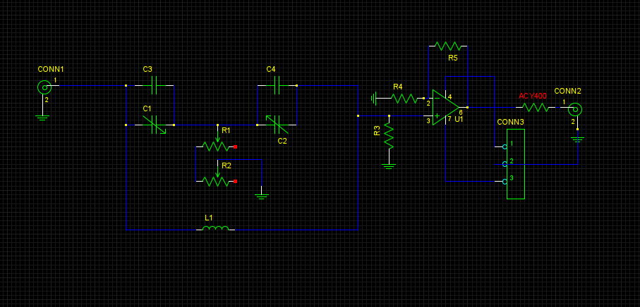
Choose Components and Build the Circuit
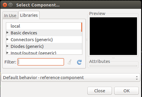
Using the Add component menu (looks like a 2 pronged power cable) select the various electronic components that will be on your board.
The filter option in this menu allows you to quickly type the part in order to find it rather than searching through the menus. (ie. ground or resistor)
Move the parts around similar to how they will be constructed on the board. This wont be the final layout, but make sure all necessary connections can be made. Then connect components by clicking the blue add nets mode button next to the add components button.
To de-select a component or a wire right click the mouse.
If you need to rotate or flip components for any reason, click on the component and then press er to rotate or ei to flip.
You can change the name and what is visible about the component by double clicking on it and changing the visibility settings and its attributes.
After the circuit is constructed and all connections are made correctly its time to add footprints to the components.
Assign Footprints
Footprints provide the information about the physical specifications of each part in the circuit such as size, number of pins, pin size... ect.
Most common circuit parts (resistors, caps,...) have pre-made footprints available, speciality parts need to have their footprints designed and saved. Once a footprint is made and saved it can be used in the future.
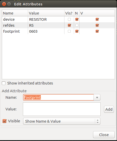
To assign a footprint to a commonly used part, double click on the component. Towards the bottom of the menu, below add attribute, select the name drop down menu. When the menu drops down, select footprint. In the value box, this is where you'll enter the code for the specific footprint needed. Common codes and naming conventions can be found at this website, [2]
After the value is entered, click add. Again keep in mind you can choose to make this footprint name not visible on the diagram. To assign the same footprint to multiple components, click on another component before closing the edit attributes menu, and again click add. This will add the previously chosen footprint to the newly selected component.
Custom Footprints
To build a custom footprint open the program pcb designer. The Via button in the lower left portion of the side bar menu corresponds to pins. Click and drag these vias where physical pins will. This requires measuring and planning on the physical component. There is mil measurements in the top right corner to tell where the cursor is so that you can be precise about where the vias are placed. Now you can highlight the entire footprint and then press (control x) this cuts the design to buffer. Then under the buffer menu, click convert buffer to element. This will place this element on the screen. Now, click and copy that element, and under the buffer menu, click save buffer to file. Save into a directory that can be accessed by gschem. In gschem for the footprint id, use whatever file name you save the custom footprint as.
Transferring to PCB Designer
When all components have a footprint and when all needed connections are made you are ready to send this blueprint to the pcb designer program. Save your file at this time(in the same directory that the custom footprints are saved to). Now in the command line use the command gsch2pcb. Make sure you are in the directory where the .sch file is. For example this is what your command line should resemble with different file names and in a directory where your file is saved. (gsch2pcb -d ~/pcb-mylib/ BridedTeePCB_preamp.sch).
When done successfully, the command line will give directions to continue. I have listed them below.
1. Run pcb on your file ie. BridedTeePCB_preamp.pcb
2. From within PCB, select File -> Load layout data to paste buffer and select BridedTeePCB_preamp.new.pcb (this will be you files name) to load the new footprints into your existing layout.
3. From within PCB, select File -> Load netlist file and select BridedTeePCB_preamp.net to load the updated netlist.
4. From within PCB, enter :ExecuteFile(BridedTeePCB_preamp.cmd) to update the pin names of all footprints.
PCB Designer
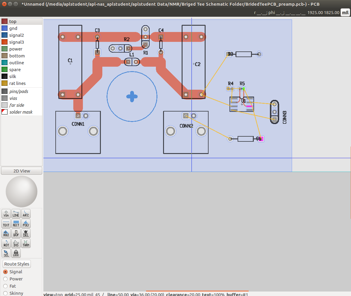
The last exercise should have transferred the information about all the needed components and connections to the PCB program. In this PCB program you will move the components by dragging and dropping them to where they will physically go on the board. The yellow rat lines connecting components show the needed connections. When you move multiple components press the o button to optimize and re-position the rats nest. Clicking on the ROT button in the bottom left menu bar allows you to click on components to rotate them. Once all components are placed where they are physically going to be on the board (allowing for the needed connections to be made) you are ready to begin drawing the copper lines. Note, if rat lines intersect that is okay, they simply show where connections need to be made. However when laying out components be aware that copper drawn in lines should not intersect unless they are meant to.
To begin drawing in copper lines first click on route styles in the bottom left corner. From there you can change the line width to you desired amount. (127 mm gives a characteristic impedance of 50 ohms). After this is selected you can zoom in and our using the mouse wheel hovering the mouse over where you would like to zoom. This is helpful where trying to see exactly where copper lines are being drawn. Next click on one of the signal tabs in the top left corner. it should highlight grey. Then click LINE in the bottom of this menu. Click to start drawing, each time clicking to change directions. When done drawing hit escape. Name another tab with GND and click on it so that it turns grey. Then with the RECT button in the bottom left, cover the entire board with a ground plane if one is needed. Then to connect components to ground, click on the THRM button in the bottom left and click the pins that will be grounded.
Printing the Transparency
After you are satisfied with the circuit make sure to save it and then go to file---> export and choose export to postscript. This provides a nice way to view each layer of the circuit before printing. Check the parody of the circuit layers in the exported postscript. If they need to be changed you can go back into the pcb program and after exporting to postscript, check the mirror option. Note, for print out transparencies you almost always want mirror selected, this is because the transparency is flipped and laid over the pcb before developing. Once you are satisfied with the post script diagrams open gimp photo editor and in gimp open the needed pages of the postscript (pgs 2 and 3 are the top and bottom). Import at 600 dpi (resolution). Print a transparency of this on a high resolution printer.


