Eeschema: Difference between revisions
Aplstudent (talk | contribs) |
Aplstudent (talk | contribs) |
||
| (3 intermediate revisions by the same user not shown) | |||
| Line 4: | Line 4: | ||
With the Eeschema window open select File -> Page settings. This will bring up a menu that allows you to title and author your schematic. In the "Title" section write the title of your project and in the "Comment4" section write "Author: Your Name". In the bottom right corner of the schematic you'll now see your name and project title. | With the Eeschema window open select File -> Page settings. This will bring up a menu that allows you to title and author your schematic. In the "Title" section write the title of your project and in the "Comment4" section write "Author: Your Name". In the bottom right corner of the schematic you'll now see your name and project title. | ||
The image below show the Eeschema page with the most commonly used tools labeled. | |||
[[File:KiCad Eeschema Window.png]] | |||
==Circuit Diagram== | ==Circuit Diagram== | ||
| Line 15: | Line 19: | ||
Once you have the "Run CvPcb to associate components and footprints" open you'll see three columns. The left column contains the different footprint libraries you can search. The middle column shows the different components which will all need to be associated. An unassociated component will look something like this: | Once you have the "Run CvPcb to associate components and footprints" open you'll see three columns. The left column contains the different footprint libraries you can search. The middle column shows the different components which will all need to be associated. An unassociated component will look something like this: | ||
1 | 1 P1 - CONN_01X02 : | ||
while the associated component above will look like this: | while the associated component above will look like this: | ||
1 | 1 P1 - CONN_01X02 : Pin_headers:Pin_Header_Straight_1x02 | ||
The component association is complete when every component in the middle column has the appropriate foot print assigned (as shown in the example above). Refer to the image below to better understand the "Run CvPcb to associate components and footprints" window. | The component association is complete when every component in the middle column has the appropriate foot print assigned (as shown in the example above). Refer to the image below to better understand the "Run CvPcb to associate components and footprints" window. | ||
| Line 31: | Line 35: | ||
If you haven't found all the footprints you need you must either create your own footprint and save it to a footprint library or download a preexisting footprint library from a trusted source. If you're making your own footprint you'll likely need to switch back and forth between Eeschema and the PCB footprint editor. You can learn all about how to make your own footprint in the [[Footprint Editor]] section. | If you haven't found all the footprints you need you must either create your own footprint and save it to a footprint library or download a preexisting footprint library from a trusted source. If you're making your own footprint you'll likely need to switch back and forth between Eeschema and the PCB footprint editor. You can learn all about how to make your own footprint in the [[Footprint Editor]] section. | ||
Now, assuming you have a footprint library you want to add (the [[ | Now, assuming you have a footprint library you want to add (the [[Footprint Editor]] section explains how to make your own), reopen the "Run CvPcb to associate components and footprints" window in Eeschema. From the dropdown menu select Prefrences -> Footprint Libraries and select "Append with Wizard". Select "Files on my computer" and click "Next". Find the path to your footprint library (this will have a .pretty suffex) and click "Next". Now press "Next" again and decide if you want to save the library to the current project or to all future projects (only save the library globally if it is properly named and you are sure the footprints are correct). Then, select "Finish". Now you're library should be appended to the list of available libraries and you can check by looking through the left column of the "Run CvPcb to associate components and footprints" window. Find your new footprints and associate it to the corresponding component. | ||
==Saving and Closing the Footprint Association== | ==Saving and Closing the Footprint Association== | ||
Latest revision as of 23:23, 4 February 2019
Opening Eeschema
The first program you'll want to use is called Eeschema this is where you'll make your circuit diagram and can be opened by clicking Tools -> Run Eeschema in the startup KiCad menu. Eeschema is a way to digitally draw the circuit diagram and is really only used to establish how your components will be connected. This means while using Eeschema we don't need to worry about how the components will physically be placed on our PCB and we should only focus on making a correct circuit diagram.
With the Eeschema window open select File -> Page settings. This will bring up a menu that allows you to title and author your schematic. In the "Title" section write the title of your project and in the "Comment4" section write "Author: Your Name". In the bottom right corner of the schematic you'll now see your name and project title.
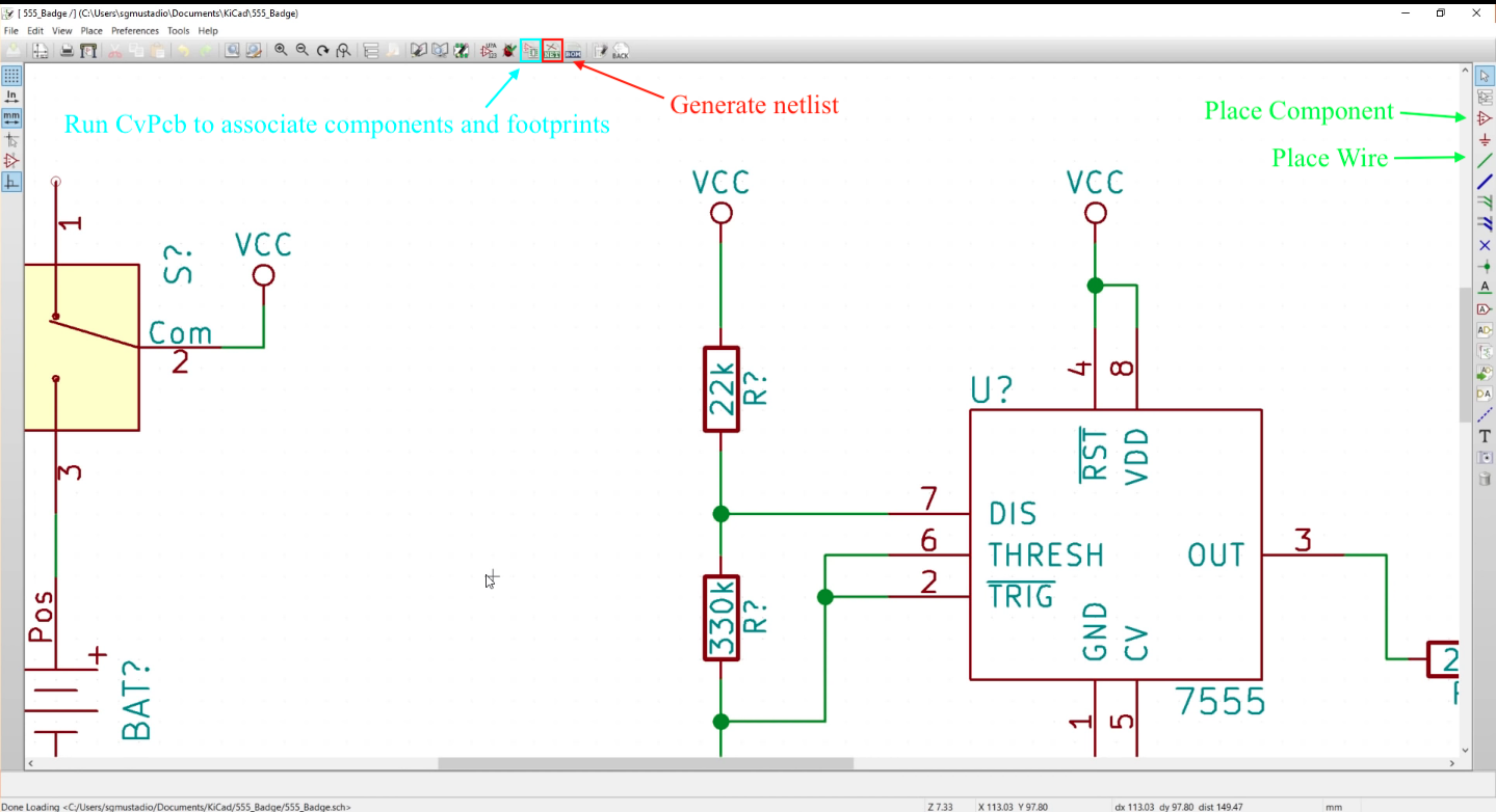
The image below show the Eeschema page with the most commonly used tools labeled.
Circuit Diagram
In Eeschema we'll want to place different components and connect them with wires. To place a new component go to the "Place" dropdown menu and select "Component" to place a component. Then double click somewhere on the schematic to bring up a list of possible components. Different components will be filtered based on your search; resistors are labeled as "R" and capacitors are "C", but more specific components can be labeled by their model number. Once you have all your components down (including Vcc and GND) you'll want to connect everything with wires. To place wires go to the "Place" dropdown menu and select wire. Connect all your components appropriately and save the file.
Footprint Association
At this point you'll begin assigning footprints to components. To do this, you'll click the red and green icon in the middle of the top toolbar labeled "Run CvPcb to associate components and footprints". Each component needs a footprint associated with it (the footprint contains the information about the physical location of pins/connections on the component, which is necessary for drilling holes in and soldering on the PCB).
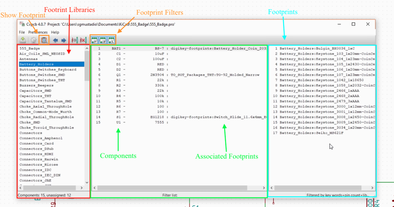
Once you have the "Run CvPcb to associate components and footprints" open you'll see three columns. The left column contains the different footprint libraries you can search. The middle column shows the different components which will all need to be associated. An unassociated component will look something like this:
1 P1 - CONN_01X02 :
while the associated component above will look like this:
1 P1 - CONN_01X02 : Pin_headers:Pin_Header_Straight_1x02
The component association is complete when every component in the middle column has the appropriate foot print assigned (as shown in the example above). Refer to the image below to better understand the "Run CvPcb to associate components and footprints" window.
The right most column is where you can find the footprints to associate with the component. The selected component will be associated with a footprint by finding and double clicking the correct footprint on the right column. Finding the correct footprint can be difficult, especially because it might not exist in the current libraries (see the next paragraph for how to add footprints and libraries), but there are a few tools which make this process easier. In the top toolbar the three most right icons (they are pictures of green and white components) that filter the results in the right column. The left most icon of the three filters the the list by keywords, the middle icon filters the list by pin count, and the right icon filters the list by the library selected. I find that the keyword filter is the most helpful. You can also bring up the footprint for any selected footprint in the right column by clicking the toolbar icon with a picture of a component under a magnifying glass (labeled as "View selected footprint"). This is very helpful to double check that you've selected the correct foot print. If you found all the footprints you needed in the preloaded libraries you can skip the next section, but if some footprints were missing you can read about adding footprint libraries below.
Adding Footprint Libraries
If you haven't found all the footprints you need you must either create your own footprint and save it to a footprint library or download a preexisting footprint library from a trusted source. If you're making your own footprint you'll likely need to switch back and forth between Eeschema and the PCB footprint editor. You can learn all about how to make your own footprint in the Footprint Editor section.
Now, assuming you have a footprint library you want to add (the Footprint Editor section explains how to make your own), reopen the "Run CvPcb to associate components and footprints" window in Eeschema. From the dropdown menu select Prefrences -> Footprint Libraries and select "Append with Wizard". Select "Files on my computer" and click "Next". Find the path to your footprint library (this will have a .pretty suffex) and click "Next". Now press "Next" again and decide if you want to save the library to the current project or to all future projects (only save the library globally if it is properly named and you are sure the footprints are correct). Then, select "Finish". Now you're library should be appended to the list of available libraries and you can check by looking through the left column of the "Run CvPcb to associate components and footprints" window. Find your new footprints and associate it to the corresponding component.
Saving and Closing the Footprint Association
After you double check that all the footprints associated to all the components are correct, save your footprint associations (File -> Save Edits), and you're ready to begin designing the physical layout of your PCB. You can close the "Run CvPcb to associate components and footprints" window by clicking File -> Close, this will bring you back to Eeschema.
Generating a Netlist
Now, we want to generate a netlist. The netlist file will contain all the information about how the different components and their footprints are connected. To create a netlist, click the "Generate netlist" icon in the Eeschema toolbar. Make sure the Pcbnew tab is selected and click generate. Name your netlist and make sure it is being saved in the project directory, then click "Save". This saves a file with a .net suffex in your project directory.
At this point we are finished with Eeschema and we'll want to continue to the next program called Pcbnew where you'll upload our netlist and design your PCB layout.

